MMI1x2: MULTIMODE INTERFERENCE COUPLER
DESCRIPTION
Summary: The MMI1x2 is a multimode interference coupler with a broad bandwidth centered at C Band.
Operational principle: This MMI has a single input port (Port 1) and two output ports (Ports 2 and 3). When light enters the input port, the power is evenly divided between the output ports, with no phase difference between them.
Performance: The nominal design performance for TE polarization shows excess losses < 1 dB covering from O to U telecommunications bands (1250nm-1750nm) and < 0.3 dB for C+L bands (1530nm-1625nm). It shows virtually no phase difference nor imbalance between output ports.
Maturity level: III-b
LAYOUT
Black Box:

Pin specifications:
Pin No. |
Width (nm) |
|---|---|
0 |
500 |
1 |
500 |
2 |
500 |
FDTD SIMULATION
This section describes the simulated performance of the building block, as well as the project conditions under which the simulations have been carried out. The results of this section have been obtained through precise 3D-FDTD simulations. Convergence tests have been carried out to ensure maximum accuracy.
Layer settings: The building block has been simulated in a SOI platform.
Layer |
Material |
Thickness |
|---|---|---|
Strip waveguide |
Si (dispersive) |
220 nm |
Cladding |
SiO2 |
semi-infinite |
BOX |
SiO2 |
semi-infinite |
COMPACT MODEL
S-matrix settings: Lumerical Interconnect reads the compact model as an N-port building block with the following ports and modes:
Port No. |
Port name |
Mode |
Port location |
|---|---|---|---|
1 |
port 1 |
1 (TE0) |
Left |
2 |
port 2 |
1 (TE0) |
Left |
3 |
port 3 |
1 (TE0) |
Right |
4 |
port 4 |
1 (TE0) |
Right |
The compact model contains the building-block performance at the following bandwidth:
Wavelength range |
|---|
1250-1750 nm |
FIGURES OF MERIT
Transmission
Excess losses

Back reflections

MONTE CARLO ANALYSIS
This section presents the Monte Carlo analysis performed to assess the effect of fabrication variations on the building block response.
SPECIFICATIONS
Besides the nominal design, four process corners have been calculated through 3D-FDTD simulations with the following width and thickness deviations (dw and dh, respectively).
Design |
dw (nm) |
dh (nm) |
|---|---|---|
nominal |
0 nm |
0 nm |
corner 1 |
+10 nm |
+5 nm |
corner 2 |
+10 nm |
-5 nm |
corner 3 |
-10 nm |
+5 nm |
corner 4 |
-10 nm |
-5 nm |
By interpolating from these designs, a Monte Carlo analysis has been performed using Gaussian statistical variation of dw and dh.
FIGURES OF MERIT
Transmission
Excess losses

Back reflections

MMI2x2 I: MULTIMODE INTERFERENCE COUPLER
DESCRIPTION
Summary: The MMI2x2 is a multimode interference coupler whose operation covers the S, C and L bands.
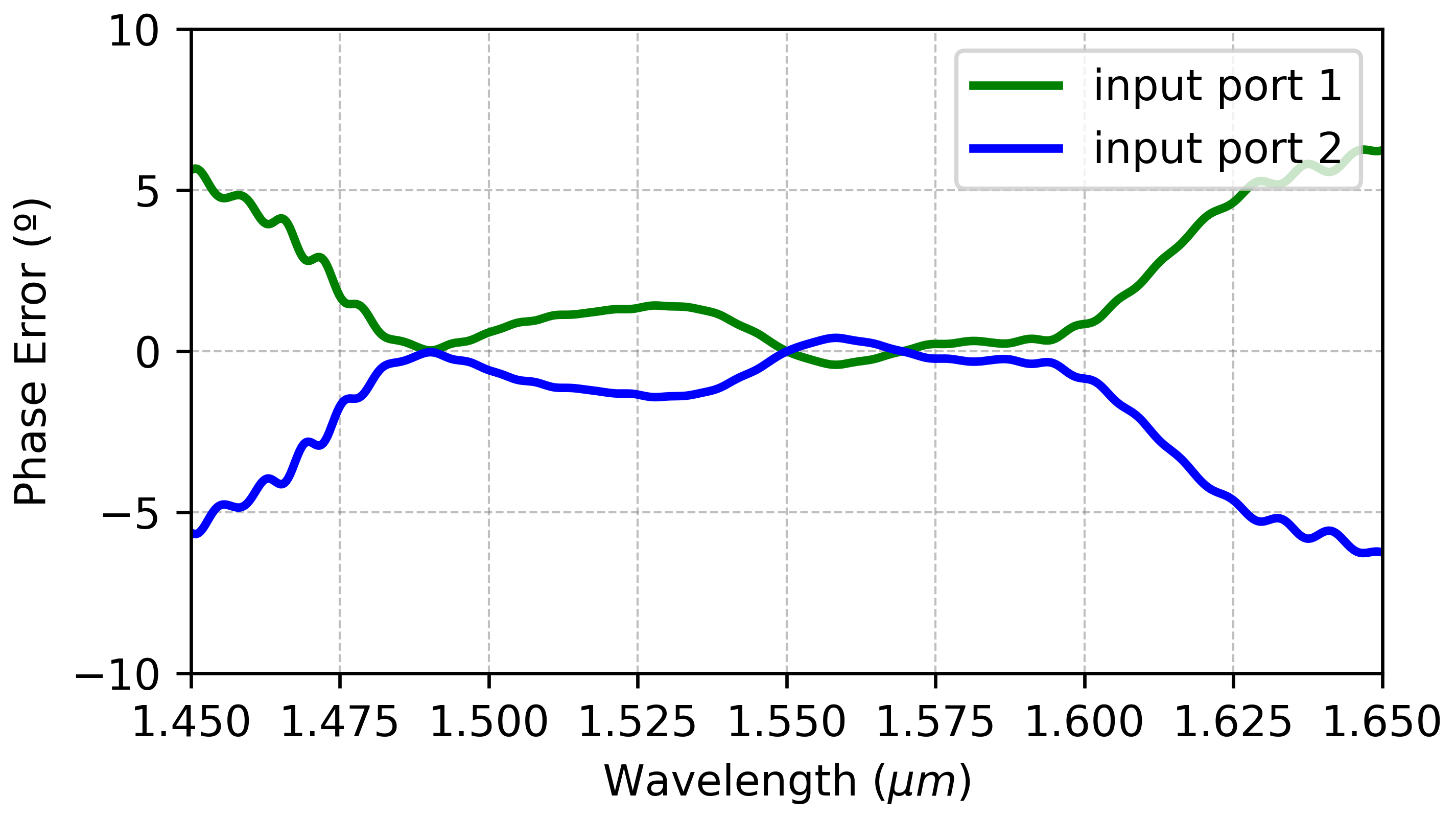
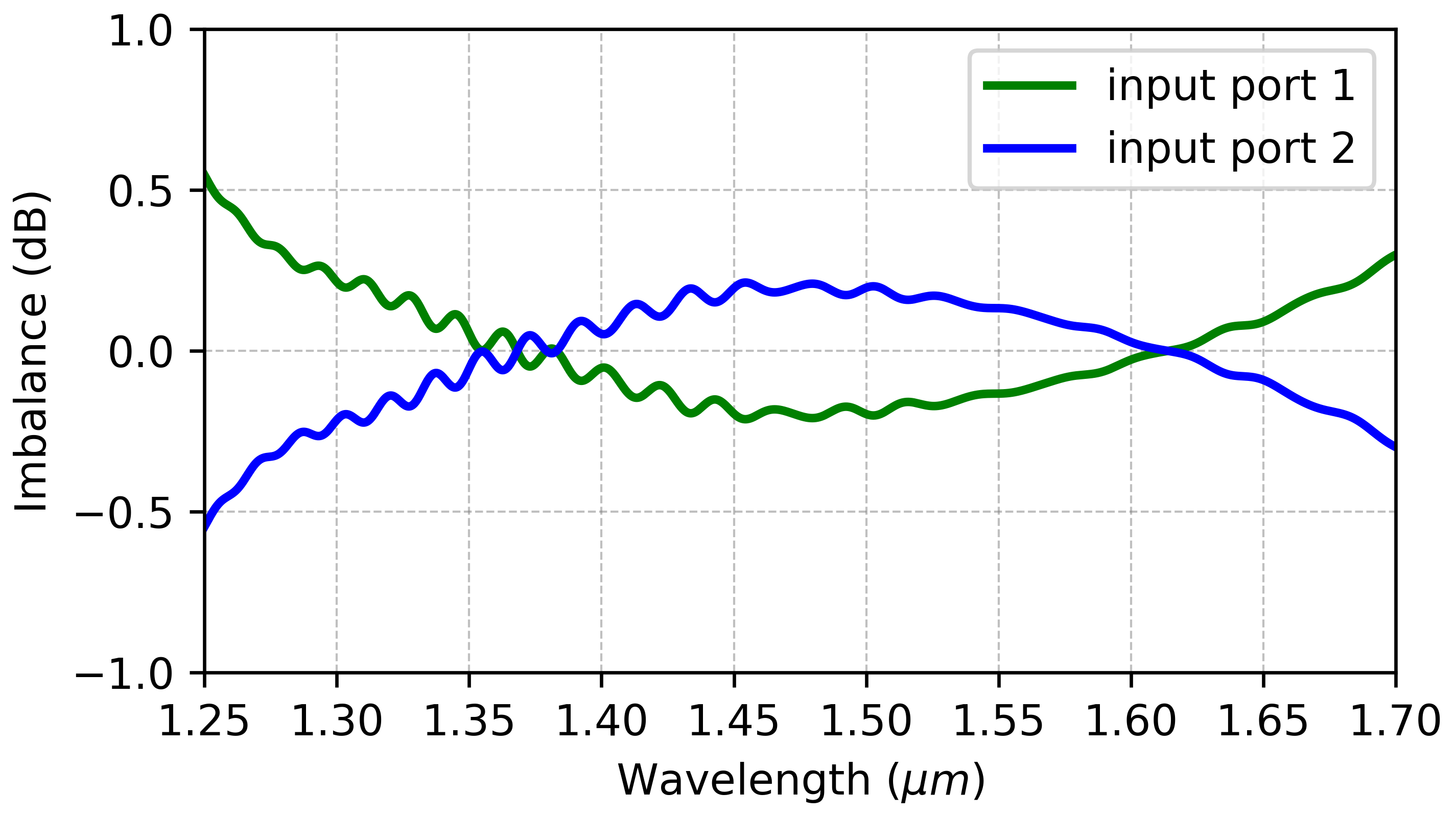
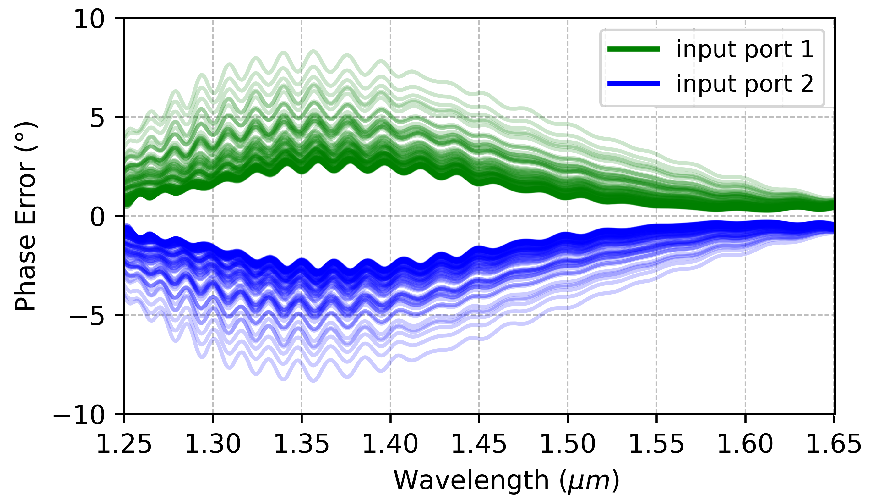
Operational principle: This MMI has two input ports (Ports 1 and 2) and two output ports (Ports 3 and 4). When ligth enters one input port, the power is equally divided between the two outputs, producing a 90º phase difference between them. The main performance indicators are defined in this document.
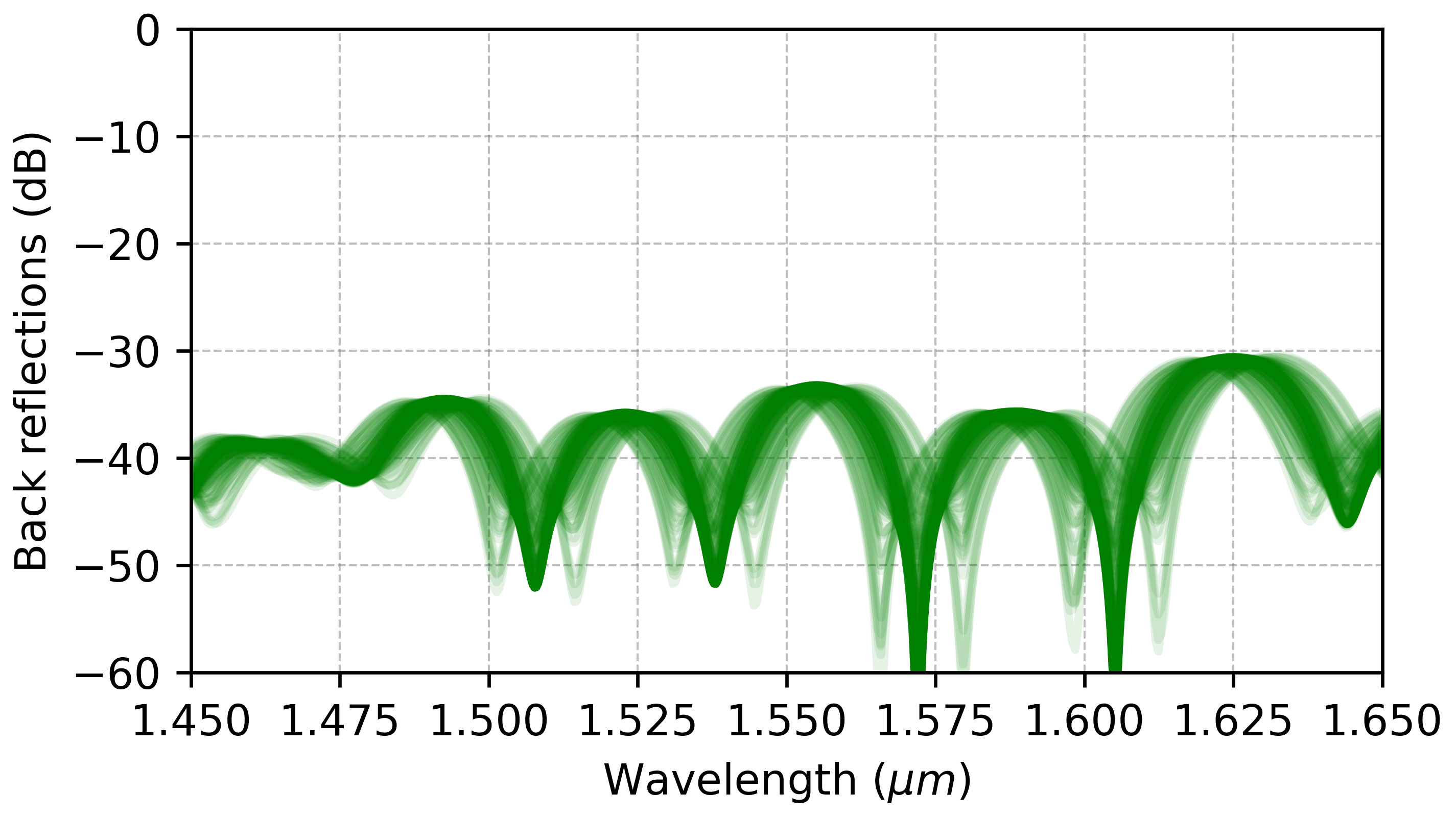
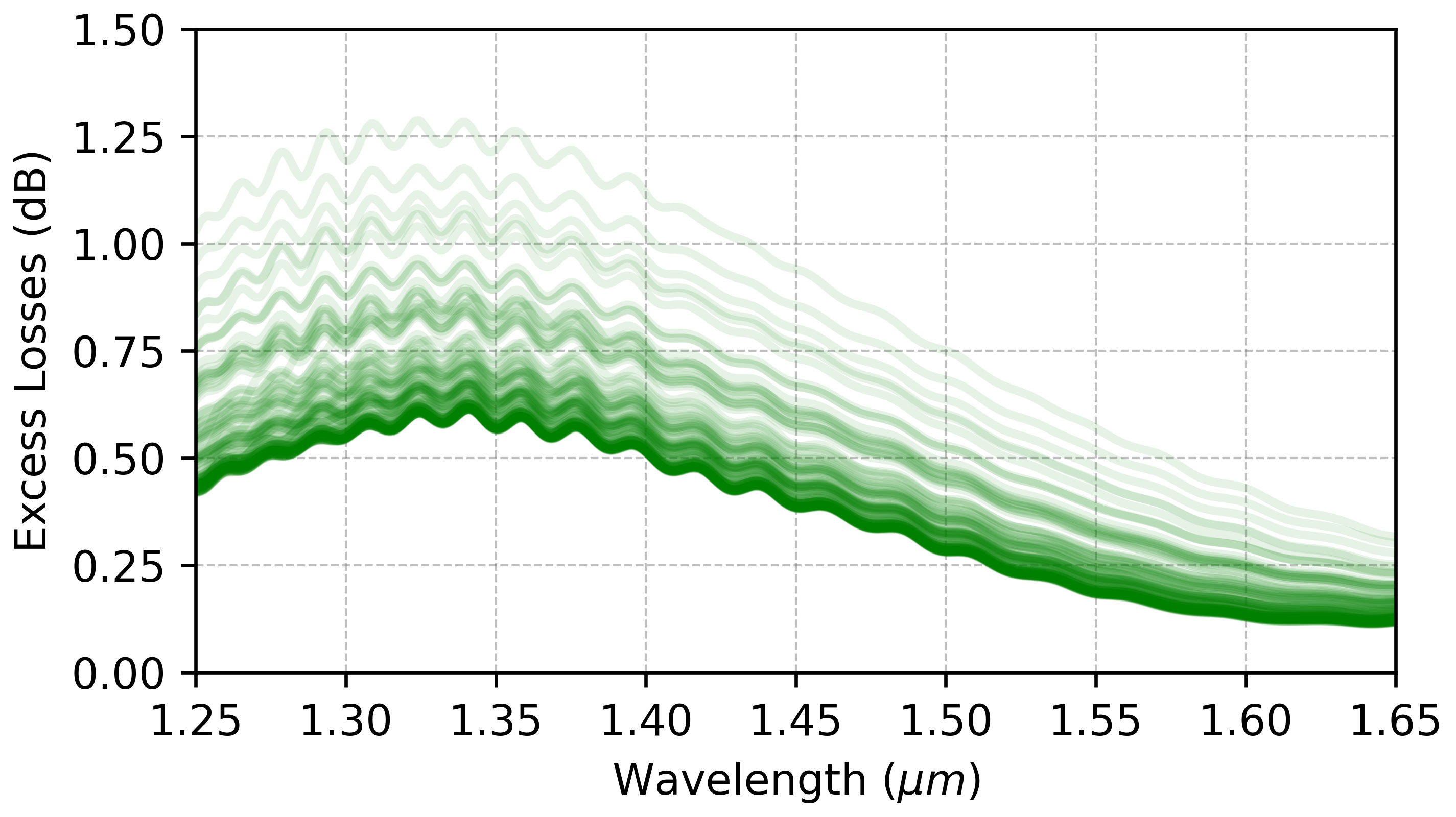
Performance: The nominal design for TE polarization presents a 170 nm wide operational bandwidth covering the S, C and L bands. Within this range, it shows excess losses and imbalance <0.5 dB, as well as 90º phase difference between output ports with a phase error <5º. Furthermore, the excess losses and phase error fall below 0.3 dB and 1.5º for C and L bands.
Maturity level: III-b
LAYOUT
Black Box:

Pin specifications:
Pin No. |
Width (nm) |
|---|---|
0 |
500 |
1 |
500 |
2 |
500 |
3 |
500 |
FDTD SIMULATION
This section describes the simulated performance of the building block, as well as the project conditions under which the simulations have been carried out. The results of this section have been obtained through precise 3D-FDTD simulations. Convergence tests have been carried out to ensure maximum accuracy.
Layer settings: The building block has been simulated in a SOI platform.
Layer |
Material |
Thickness |
|---|---|---|
Strip waveguide |
Si (dispersive) |
220 nm |
Cladding |
SiO2 |
semi-infinite |
BOX |
SiO2 |
semi-infinite |
COMPACT MODEL
S-matrix settings: Lumerical Interconnect reads the compact model as an N-port building block with the following ports and modes:
Port No. |
Port name |
Mode |
Port location |
|---|---|---|---|
1 |
port 1 |
1 (TE0) |
Left |
2 |
port 2 |
1 (TE0) |
Left |
3 |
port 3 |
1 (TE0) |
Right |
4 |
port 4 |
1 (TE0) |
Right |
The compact model contains the building-block performance at the following bandwidth:
Wavelength range |
|---|
1350-1750 nm |
FIGURES OF MERIT
Transmission
Imbalance

Excess losses

Phase error
Back reflections

MONTE CARLO ANALYSIS
This section presents the Monte Carlo analysis performed to assess the effect of fabrication variations on the building block response.
SPECIFICATIONS
Besides the nominal design, four process corners have been calculated through 3D-FDTD simulations with the following width and thickness deviations (dw and dh, respectively).
Design |
dw (nm) |
dh (nm) |
|---|---|---|
nominal |
0 nm |
0 nm |
corner 1 |
+10 nm |
+5 nm |
corner 2 |
+10 nm |
-5 nm |
corner 3 |
-10 nm |
+5 nm |
corner 4 |
-10 nm |
-5 nm |
By interpolating from these designs, a Monte Carlo analysis has been performed using Gaussian statistical variation of dw and dh.
FIGURES OF MERIT
Transmission
Imbalance

Excess losses

Phase error

Back reflections

MMI2x2 II: MULTIMODE INTERFERENCE COUPLER
DESCRIPTION
Summary: The MMI2x2 II is a multimode interference coupler which presents an ultra-broadband operation centered at the C-band.
Operational principle: This MMI has two input ports (Ports 1 and 2) and two output ports (Ports 3 and 4). When ligth enters one input port, the power is equally divided between the two output ports, producing a 90º phase difference between them.
Performance: The nominal design for TE polarization shows more than 400 nm of operational bandwidth with imbalance better than ±0.5 dB and excess losses <0.6 dB, as well as 90º phase difference between output ports with a phase error <2.5º.
Maturity level: III-b
LAYOUT
Black Box:

Pin specifications:
Pin No. |
Width (nm) |
|---|---|
0 |
500 |
1 |
500 |
2 |
500 |
3 |
500 |
FDTD SIMULATION
This section describes the simulated performance of the building block, as well as the project conditions under which the simulations have been carried out. The results of this section have been obtained through precise 3D-FDTD simulations. Convergence tests have been carried out to ensure maximum accuracy.
Layer settings: The building block has been simulated in a SOI platform.
Layer |
Material |
Thickness |
|---|---|---|
Strip waveguide |
Si (dispersive) |
220 nm |
Cladding |
SiO2 |
semi-infinite |
BOX |
SiO2 |
semi-infinite |
COMPACT MODEL
S-matrix settings: Lumerical Interconnect reads the compact model as an N-port building block with the following ports and modes:
Port No. |
Port name |
Mode |
Port location |
|---|---|---|---|
1 |
port 1 |
1 (TE0) |
Left |
2 |
port 2 |
1 (TE0) |
Left |
3 |
port 3 |
1 (TE0) |
Right |
4 |
port 4 |
1 (TE0) |
Right |
The compact model contains the building-block performance at the following bandwidth:
Wavelength range |
|---|
1250-1700 nm |
FIGURES OF MERIT
Transmission
Imbalance
Excess losses

Phase error

Back reflections

MONTE CARLO ANALYSIS
This section presents the Monte Carlo analysis performed to assess the effect of fabrication variations on the building block response.
SPECIFICATIONS
Besides the nominal design, four process corners have been calculated through 3D-FDTD simulations with the following width and thickness deviations (dw and dh, respectively).
Design |
dw (nm) |
dh (nm) |
|---|---|---|
nominal |
0 nm |
0 nm |
corner 1 |
+10 nm |
+5 nm |
corner 2 |
+10 nm |
-5 nm |
corner 3 |
-10 nm |
+5 nm |
corner 4 |
-10 nm |
-5 nm |
By interpolating from these designs, a Monte Carlo analysis has been performed using Gaussian statistical variation of dw and dh.
FIGURES OF MERIT
Transmission
Imbalance

Excess losses
Phase error
Back reflections

DC: DIRECTIONAL COUPLER
DESCRIPTION
Summary: This DC is a directional coupler whose operation covers the C, L and U bands with a compact footprint.
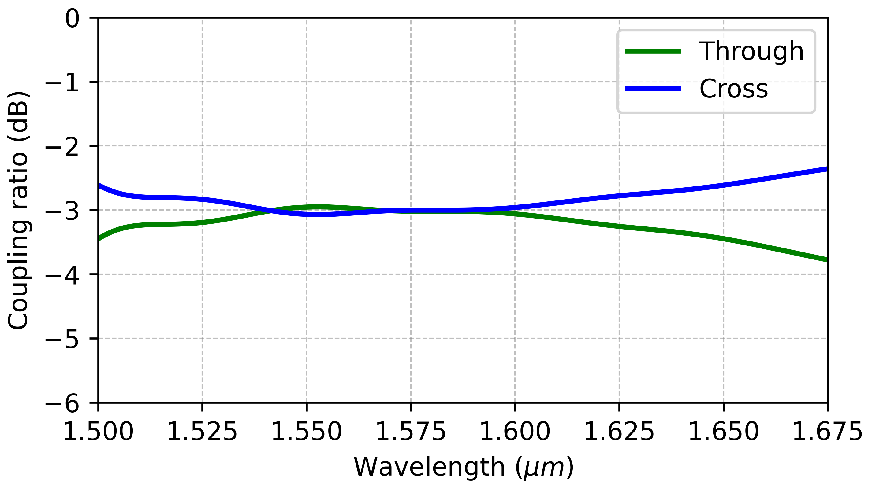
Operational principle: This design has two input ports (Ports 1 and 2) and two output ports (Ports 3 and 4). When light enters one input port, the power is equally divided between the through and cross ports. Different coupling ratios ranging from 8% to 100% are available upon request.
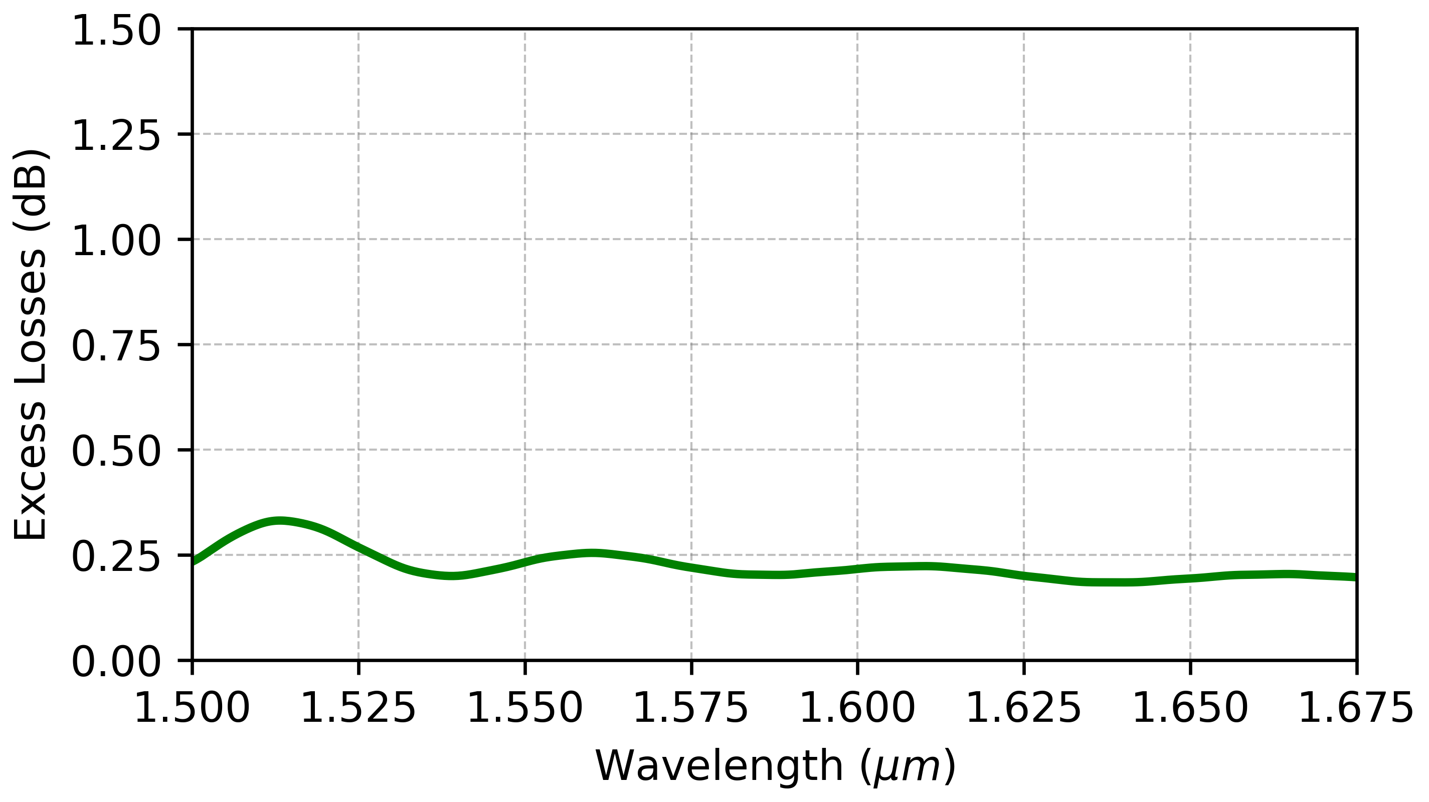
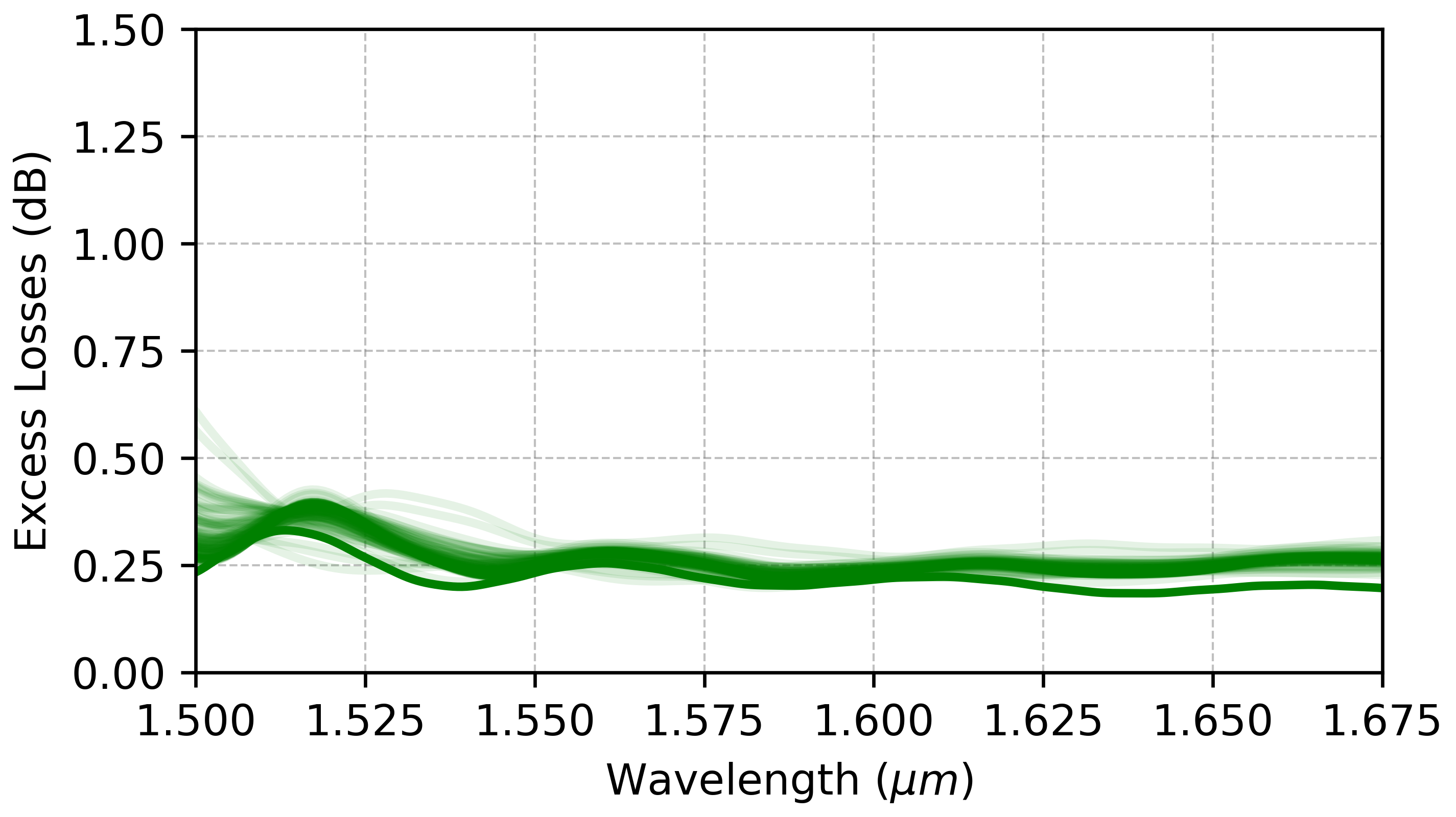
Performance: The nominal design for TE polarization presents an operational bandwidth of more than 145 nm considering a coupling ratio deviation below ±0.5 dB and excess losses around 0.25 dB.
Maturity level: III-b
LAYOUT
Black Box:

Pin specifications:
Pin No. |
Width (nm) |
|---|---|
0 |
500 |
1 |
500 |
2 |
500 |
3 |
500 |
FDTD SIMULATION
This section describes the simulated performance of the building block, as well as the project conditions under which the simulations have been carried out. The results of this section have been obtained through precise 3D-FDTD simulations. Convergence tests have been carried out to ensure maximum accuracy.
Layer settings: The building block has been simulated in a SOI platform.
Layer |
Material |
Thickness |
|---|---|---|
Strip waveguide |
Si (dispersive) |
220 nm |
Cladding |
SiO2 |
semi-infinite |
BOX |
SiO2 |
semi-infinite |
COMPACT MODEL
S-matrix settings: Lumerical Interconnect reads the compact model as an N-port building block with the following ports and modes:
Port No. |
Port name |
Mode |
Port location |
|---|---|---|---|
1 |
port 1 |
1 (TE0) |
Left |
2 |
port 2 |
1 (TE0) |
Left |
3 |
port 3 |
1 (TE0) |
Right |
4 |
port 4 |
1 (TE0) |
Right |
The compact model contains the building-block performance at the following bandwidth:
Wavelength range |
|---|
1350-1750 nm |
FIGURES OF MERIT
Transmission
Coupling ratio
Excess losses
MONTE CARLO ANALYSIS
This section presents the Monte Carlo analysis performed to assess the effect of fabrication variations on the building block response.
SPECIFICATIONS
Besides the nominal design, four process corners have been calculated through 3D-FDTD simulations with the following width and thickness deviations (dw and dh, respectively).
Design |
dw (nm) |
dh (nm) |
|---|---|---|
nominal |
0 nm |
0 nm |
corner 1 |
+10 nm |
+5 nm |
corner 2 |
+10 nm |
-5 nm |
corner 3 |
-10 nm |
+5 nm |
corner 4 |
-10 nm |
-5 nm |
By interpolating from these designs, a Monte Carlo analysis has been performed using Gaussian statistical variation of dw and dh.
FIGURES OF MERIT
Transmission
Coupling ratio

Excess losses
DC TE & TM: DIRECTIONAL COUPLER
DESCRIPTION
Summary: This broadband directional coupler is a 2x2 3dB power splitter with polarization independent response. It works over a wide bandwidth centered at the C band.
Operational principle: This design has two input ports (Ports 1 and 2) and two output ports (Ports 3 and 4). When light enters one input port, the power is equally divided between the through and cross ports. The device operates for both TE0 and TM0 polarizations.
Performance: For TE polarization, the nominal design shows a coupling ratio deviation below ±0.5 dB over a broad bandwidth of 350 nm (from 1.40 um to 1.75 um). The excess losses are below 0.25 dB for all the bandwidth, remaining below 0.04 dB for C+L bands. For TM polarization, the nominal design exhibits a coupling ratio deviation below ±0.5 dB across from 1500 nm to 1650 nm. The excess losses are below 0.5 dB within the same range and below 0.3 dB for C and L bands.
Maturity level: III-b
LAYOUT
Black Box:

Pin specifications:
Pin No. |
Width (nm) |
|---|---|
0 |
500 |
1 |
500 |
2 |
500 |
3 |
500 |
FDTD SIMULATION
This section describes the simulated performance of the building block, as well as the project conditions under which the simulations have been carried out. The results of this section have been obtained through precise 3D-FDTD simulations. Convergence tests have been carried out to ensure maximum accuracy.
Layer settings: The building block has been simulated in a SOI platform.
Layer |
Material |
Thickness |
|---|---|---|
Strip waveguide |
Si (dispersive) |
220 nm |
Cladding |
SiO2 |
semi-infinite |
BOX |
SiO2 |
semi-infinite |
COMPACT MODEL
S-matrix settings: Lumerical Interconnect reads the compact model as an N-port building block with the following ports and modes:
Port No. |
Port name |
Mode |
Port location |
|---|---|---|---|
1 |
port 1 |
1 (TE0),2 (TM0) |
Left |
2 |
port 2 |
1 (TE0),2 (TM0) |
Left |
3 |
port 3 |
1 (TE0),2 (TM0) |
Right |
4 |
port 4 |
1 (TE0),2 (TM0) |
Right |
The compact model contains the building-block performance at the following bandwidth:
Wavelength range |
|---|
1350-1750 nm |
FIGURES OF MERIT
Transmission for TE polarization
Coupling ratio for TE polarization

Excess losses for TE polarization

Transmission for TM polarization
Coupling ratio for TM polarization

Excess losses for TM polarization

MONTE CARLO ANALYSIS
This section presents the Monte Carlo analysis performed to assess the effect of fabrication variations on the building block response.
SPECIFICATIONS
Besides the nominal design, four process corners have been calculated through 3D-FDTD simulations with the following width and thickness deviations (dw and dh, respectively).
Design |
dw (nm) |
dh (nm) |
|---|---|---|
nominal |
0 nm |
0 nm |
corner 1 |
+10 nm |
+5 nm |
corner 2 |
+10 nm |
-5 nm |
corner 3 |
-10 nm |
+5 nm |
corner 4 |
-10 nm |
-5 nm |
By interpolating from these designs, a Monte Carlo analysis has been performed using Gaussian statistical variation of dw and dh.
FIGURES OF MERIT
Transmission for TE polarization
Coupling ratio for TE polarization

Excess losses for TE polarization

Transmission for TM polarization
Coupling ratio for TM polarization

Excess losses for TM polarization

MDM I: MODE DIVISION MULTIPLEXER AND MODE CONVERTER
DESCRIPTION
Summary: The mode division multiplexer is a broadband solution for (de)multiplexation, whose operation is centered at the C band. Mode division multiplexing presents an additional route towards the enhancement of bandwidth capacity. This technology enables the transmission and reception of several spatial encoded modes through a multimode waveguide, where each eigenmode is exploited as an independent data channel. This building block can be also used as a very efficient mode converter over a wide range of wavelengths.
Operational principle: When the device works as a (mode) multiplexer, the TE0 signals at Port 1 and Port 2 become multiplexed at Port 3 as one TE1 signal and one TE0 signal, respectively. The device works as a (mode) demultiplexer in the opposite direction.
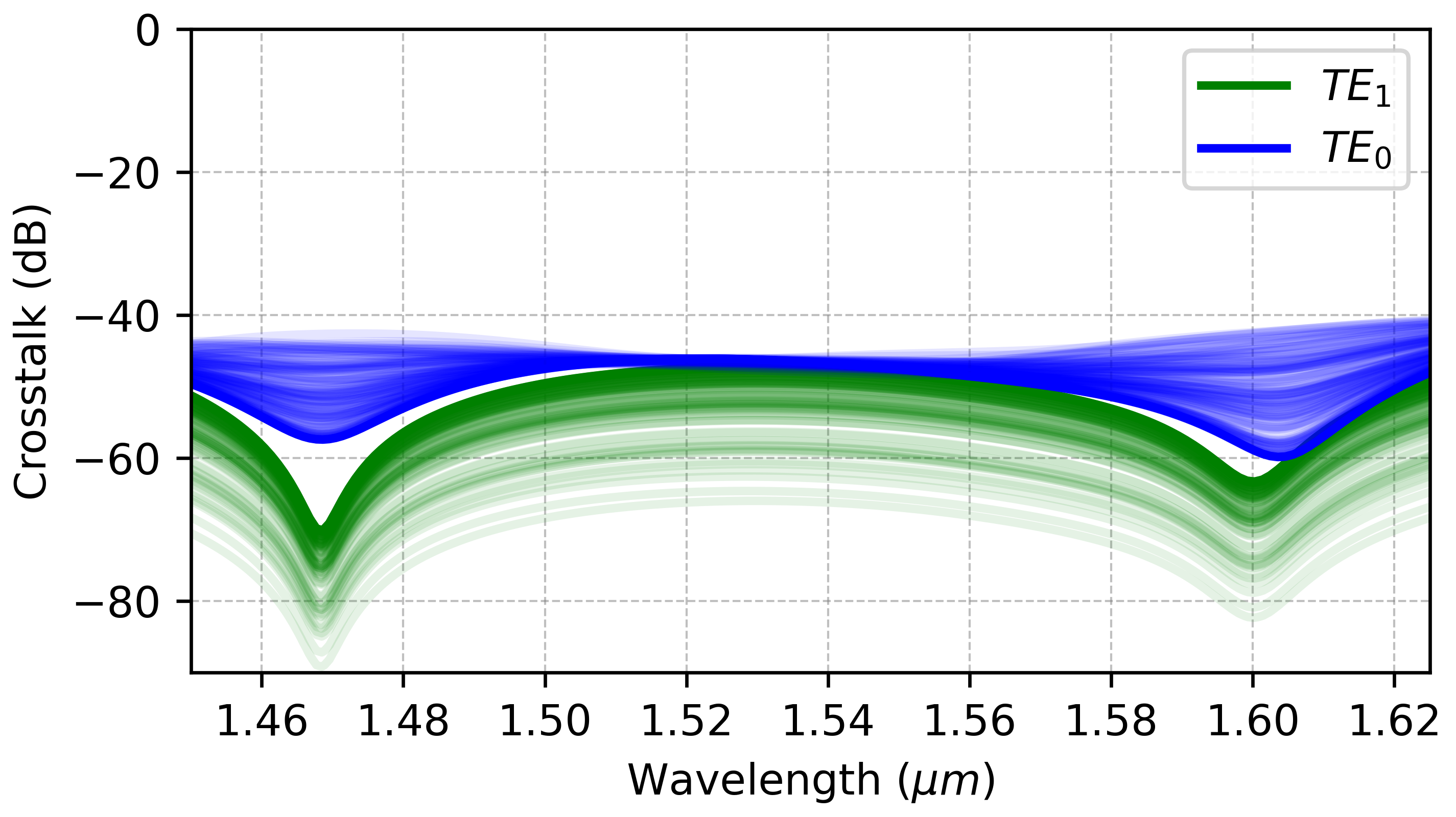
Performance: The nominal design presents a TE0-TE1 mode conversion efficiency above above 80% from 1450 nm to 1625 nm and higher than 98% for the C band. This represents conversion losses below 1 dB and 0.05 dB, respectively. The design also presents a very low crosstalk for both TE0 and TE1 below -40 dB.
For a given mode at Port 3, the crosstalk is the transmission ratio between the undesired and desired mode conversion. For instance, the TE0 crosstalk is defined as the remaining TE0 not converted to TE1 from Port 1 divided by the transmitted TE0 from Port 2. The TE1 crosstalk is the undesired TE1 generated from Port 2 divided by the TE1 excited from the TE0 at Port 1.
The overall performance improves when focusing on specific bands.
Maturity level: III-b
LAYOUT
Black Box:

Pin specifications:
Pin No. |
Width (nm) |
|---|---|
0 |
500 |
1 |
500 |
2 |
850 |
FDTD SIMULATION
This section describes the simulated performance of the building block, as well as the project conditions under which the simulations have been carried out. The results of this section have been obtained through precise 3D-FDTD simulations. Convergence tests have been carried out to ensure maximum accuracy.
Layer settings: The building block has been simulated in a SOI platform.
Layer |
Material |
Thickness |
|---|---|---|
Strip waveguide |
Si (dispersive) |
220 nm |
Cladding |
SiO2 |
semi-infinite |
BOX |
SiO2 |
semi-infinite |
COMPACT MODEL
S-matrix settings: Lumerical Interconnect reads the compact model as an N-port building block with the following ports and modes:
Port No. |
Port name |
Mode |
Port location |
|---|---|---|---|
1 |
port 1 |
1 (TE0) |
Left |
2 |
port 2 |
1 (TE0), 2 (TM0), 3 (TE1) |
Left |
3 |
port 3 |
1 (TE0), 2 (TM0), 3 (TE1), 4 (TM1) |
Right |
The compact model contains the building-block performance at the following bandwidth:
Wavelength range |
|---|
1350-1750 nm |
FIGURES OF MERIT
Conversion efficiency

Conversion loss

Crosstalk

MONTE CARLO ANALYSIS
This section presents the Monte Carlo analysis performed to assess the effect of fabrication variations on the building block response.
SPECIFICATIONS
Besides the nominal design, four process corners have been calculated through 3D-FDTD simulations with the following width and thickness deviations (dw and dh, respectively).
Design |
dw (nm) |
dh (nm) |
|---|---|---|
nominal |
0 nm |
0 nm |
corner 1 |
+10 nm |
+5 nm |
corner 2 |
+10 nm |
-5 nm |
corner 3 |
-10 nm |
+5 nm |
corner 4 |
-10 nm |
-5 nm |
By interpolating from these designs, a Monte Carlo analysis has been performed using Gaussian statistical variation of dw and dh.
FIGURES OF MERIT
Conversion efficiency

Conversion loss

Crosstalk
MDM II: MODE DIVISION MULTIPLEXER AND MODE CONVERTER
DESCRIPTION
Summary: This mode division multiplexer exhibits an ultra-broadband operation centered at the C band. Mode division multiplexing presents an additional route towards the enhancement of bandwidth capacity. This technology enables the transmission and reception of several spatial encoded modes through a multimode waveguide, where each eigenmode is exploited as an independent data channel. This building block can be also used as a very efficient mode converter over a wide range of wavelengths.
Operational principle: When the device works as a (mode) multiplexer, the TE0 signals at Port 2 and Port 3 become multiplexed at Port 1 as one TE0 signal and one TE1 signal, respectively. The device works as a (mode) demultiplexer in the opposite direction.
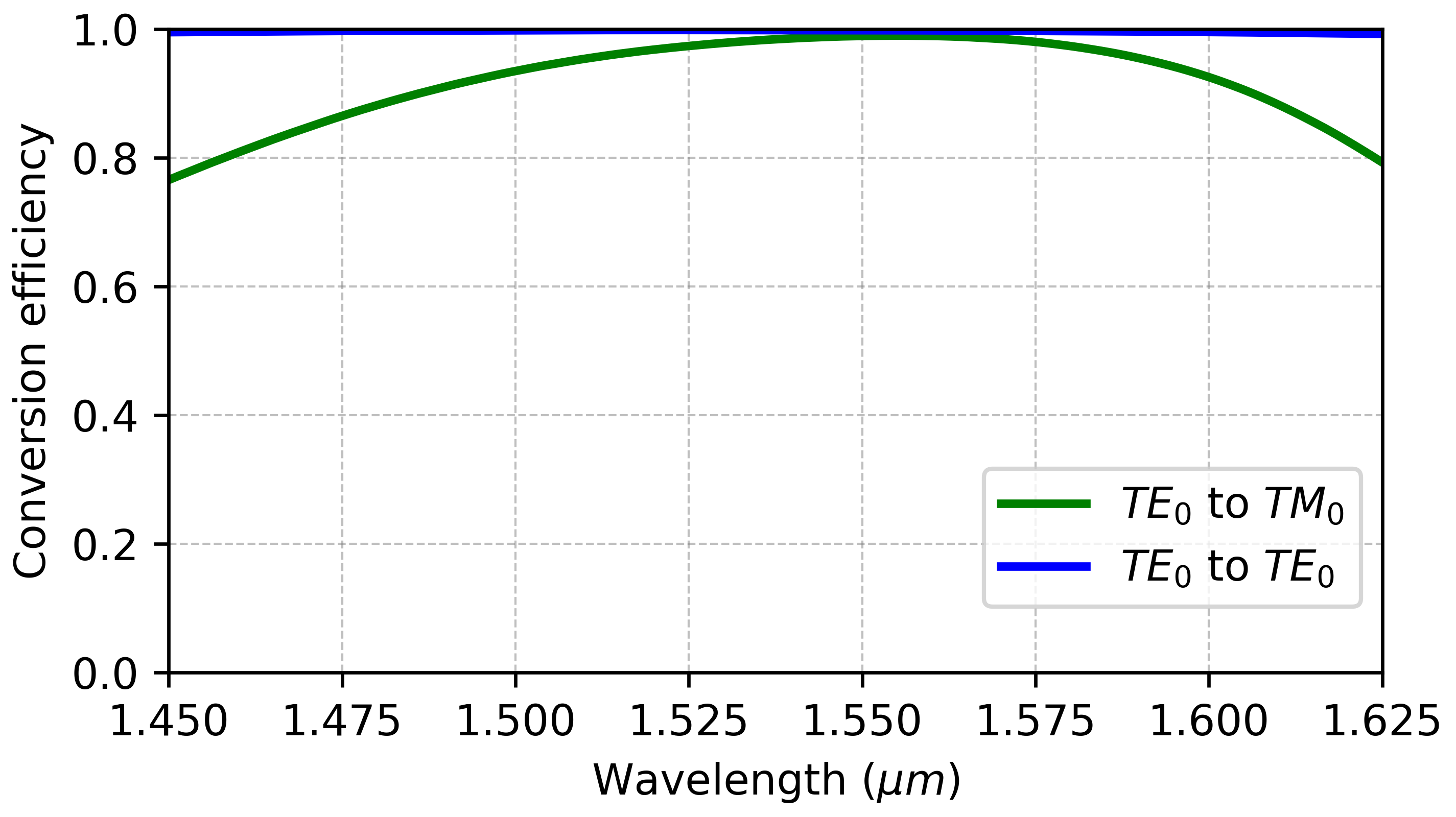
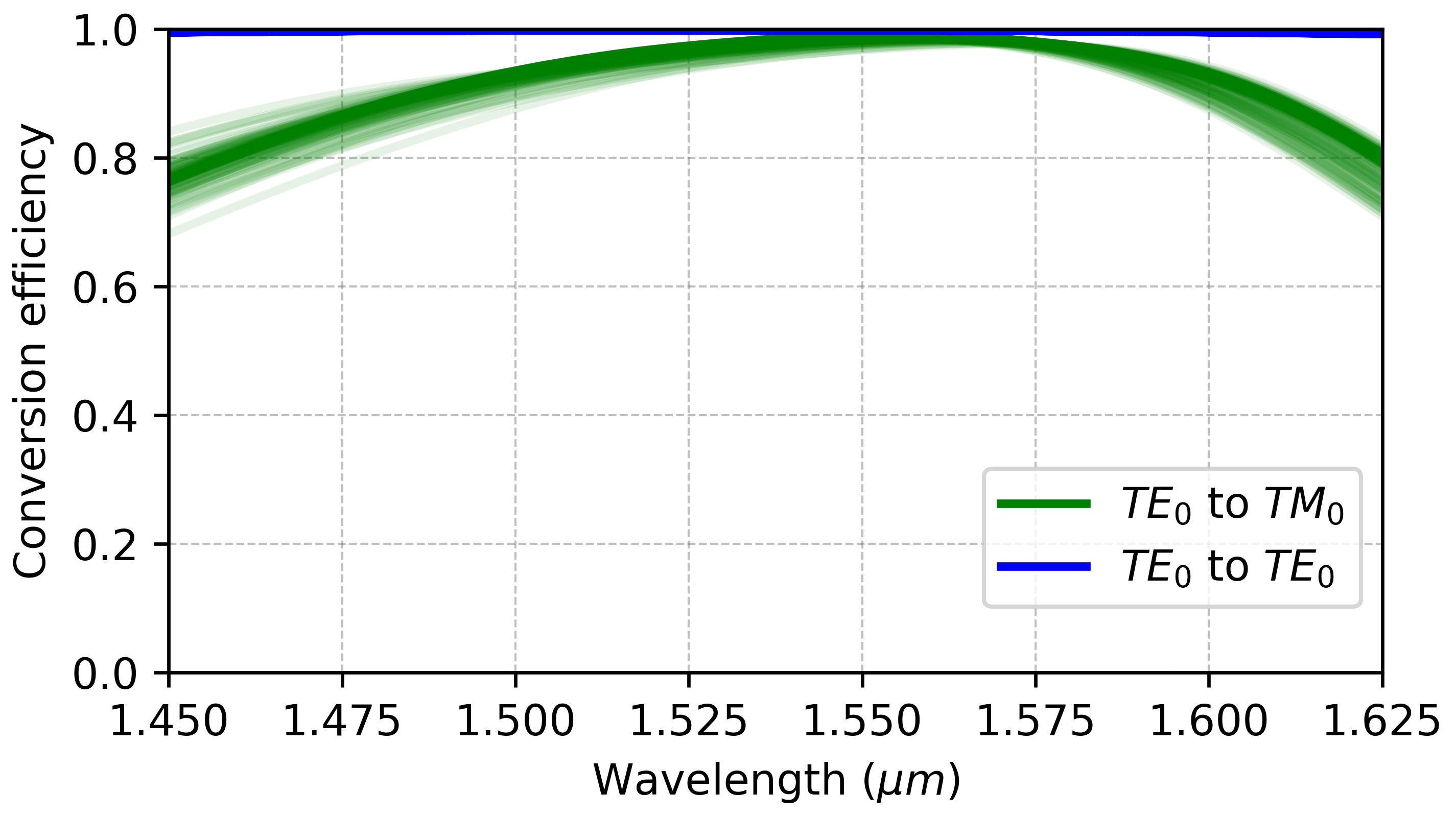
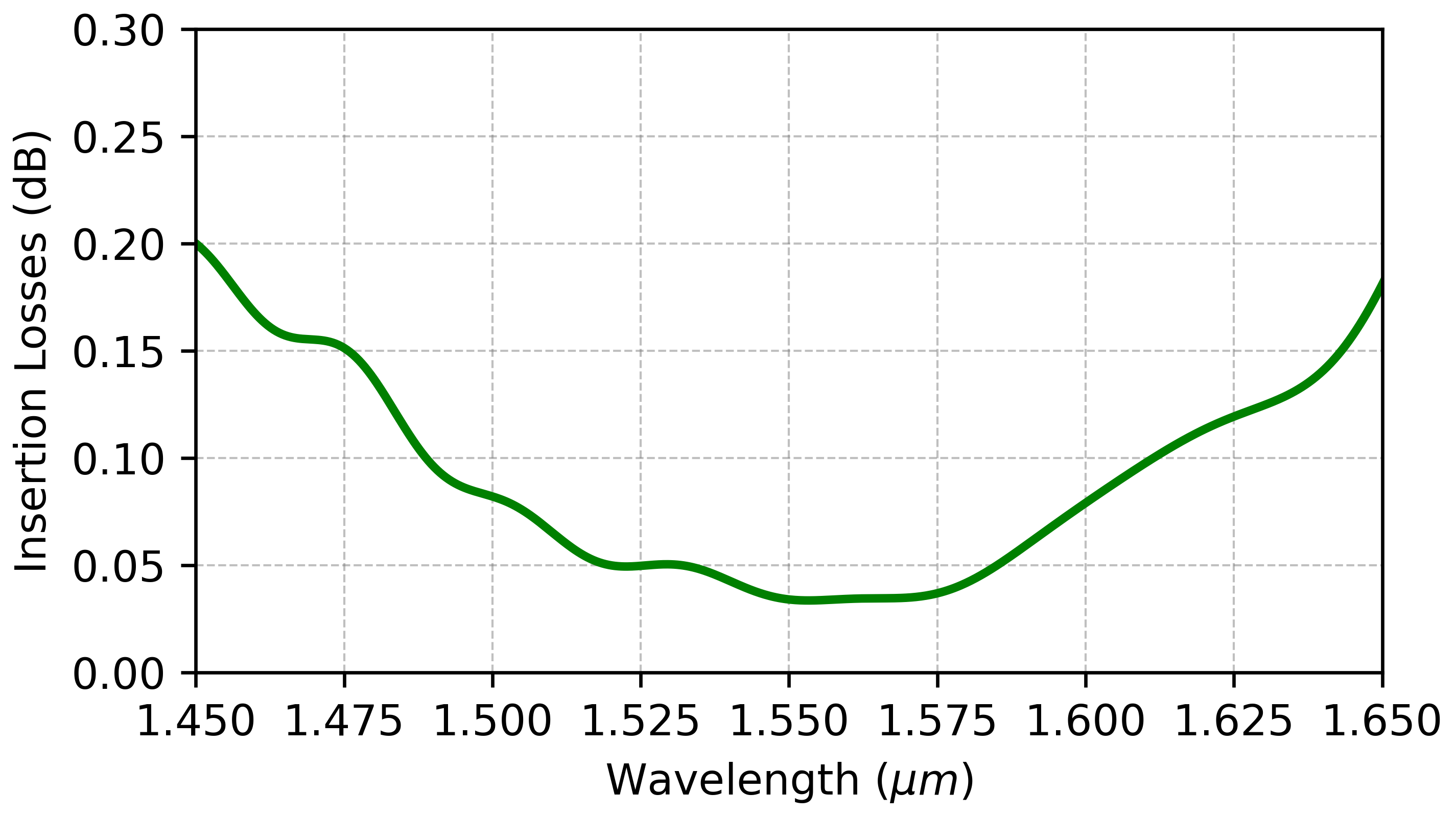
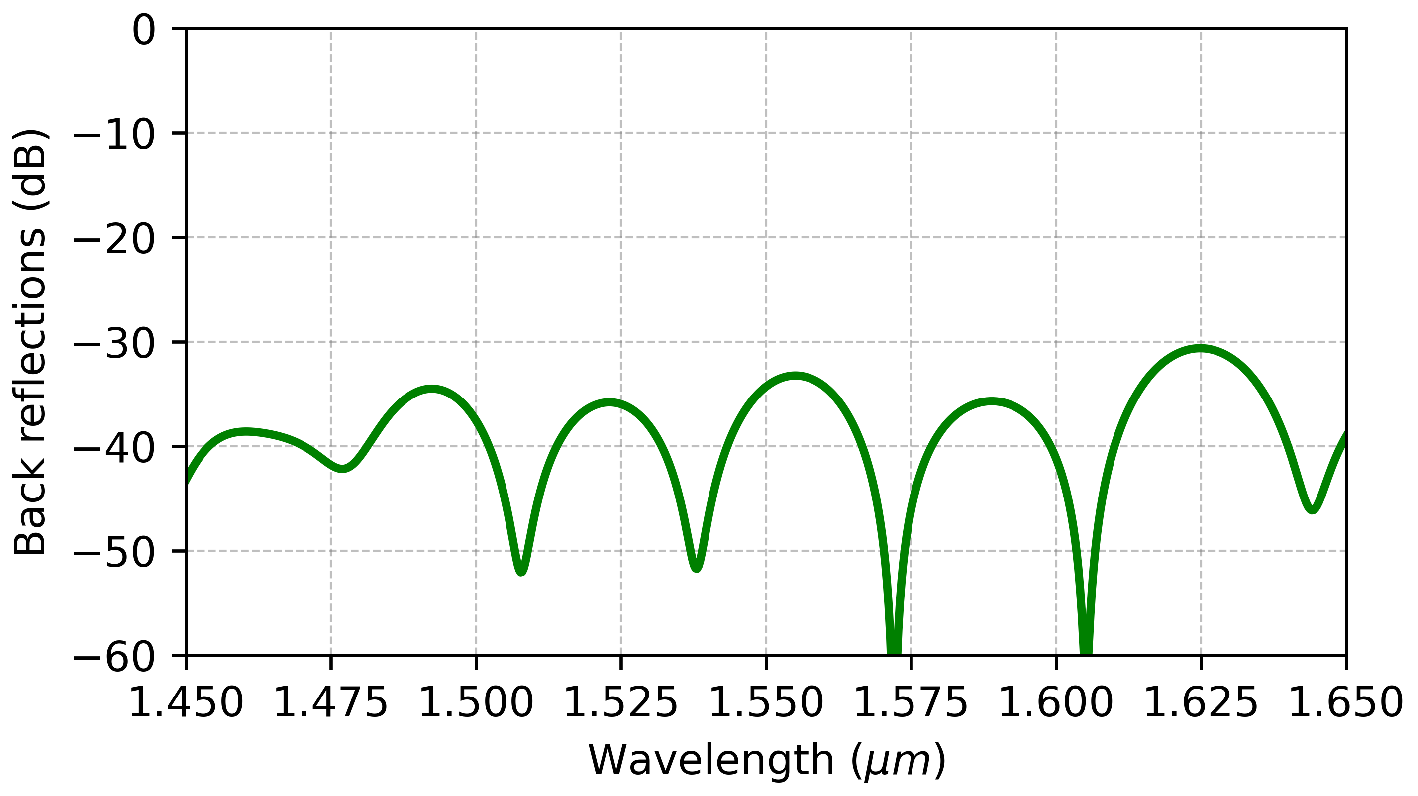
Performance: The nominal design presents a TE0-TE1 mode conversion efficiency above above 90% from 1450 nm to 1625 nm and higher than 92% for the C and L bands. This translates as a broad operation band of conversion losses below 0.5 dB from 1450 nm to 1625 nm. The design also presents a very low crosstalk for both TE0 and TE1 below -30 dB.
For a given mode at Port 1, the crosstalk is the transmission ratio between the undesired and desired mode conversion. For instance, in multiplexing configuration, the TE0 crosstalk is defined as the remaining TE0 not converted to TE1 from Port 3 divided by the transmitted TE0 from Port 2. The TE1 crosstalk is the undesired TE1 generated from Port 2 divided by the TE1 excited from the TE0 at Port 3.
The overall performance improves when focusing on specific bands.
Maturity level: III-a
LAYOUT
Black Box:

Pin specifications:
Pin No. |
Width (nm) |
|---|---|
0 |
850 |
1 |
500 |
2 |
500 |
FDTD SIMULATION
This section describes the simulated performance of the building block, as well as the project conditions under which the simulations have been carried out. The results of this section have been obtained through precise 3D-FDTD simulations. Convergence tests have been carried out to ensure maximum accuracy.
Layer settings: The building block has been simulated in a SOI platform.
Layer |
Material |
Thickness |
|---|---|---|
Strip waveguide |
Si (dispersive) |
220 nm |
Cladding |
SiO2 |
semi-infinite |
BOX |
SiO2 |
semi-infinite |
COMPACT MODEL
S-matrix settings: Lumerical Interconnect reads the compact model as an N-port building block with the following ports and modes:
Port No. |
Port name |
Mode |
Port location |
|---|---|---|---|
1 |
port 1 |
1 (TE0), 3 (TE1) |
Left |
2 |
port 2 |
1 (TE0), 3 (TE1) |
Right |
3 |
port 3 |
1 (TE0), 3 (TE1) |
Right |
The compact model contains the building-block performance at the following bandwidth:
Wavelength range |
|---|
1400-1700 nm |
FIGURES OF MERIT
Conversion efficiency

Conversion loss

Crosstalk

MONTE CARLO ANALYSIS
The Monte Carlo analysis about the effect of fabrication deviations on the device response is under progress and will be available soon.
PBS: POLARIZATION BEAM SPLITTER
DESCRIPTION
Summary: The PBS is a polarization beam splitter that exhibits a broadband operation centered at the C band.
Operational principle: This design presents one input port (Port 1) and two output ports (Ports 2 and 3). When the input port is excited with bot polarizations (TE0 + TM0), both orthogonal polarizations are separated at the output ports, in such a way that the TE0 polarization emerges through Port 2 and the TM0 through Port 3.
Performance: The nominal design performance displays 175 nm operational bandwidth with insertion losses below 1 dB and below 0.2 dB for TE0 and TM0, respectively, and extinction ratios <-20dB for both TE0 and TM0 polarizations. Such range covers the S, C and L bands.
Maturity level: III-b
LAYOUT
Black Box:

Pin specifications:
Pin No. |
Width (nm) |
|---|---|
0 |
500 |
1 |
500 |
2 |
500 |
FDTD SIMULATION
This section describes the simulated performance of the building block, as well as the project conditions under which the simulations have been carried out. The results of this section have been obtained through precise 3D-FDTD simulations. Convergence tests have been carried out to ensure maximum accuracy.
Layer settings: The building block has been simulated in a SOI platform.
Layer |
Material |
Thickness |
|---|---|---|
Strip waveguide |
Si (dispersive) |
220 nm |
Cladding |
SiO2 |
semi-infinite |
BOX |
SiO2 |
semi-infinite |
COMPACT MODEL
S-matrix settings: Lumerical Interconnect reads the compact model as an N-port building block with the following ports and modes:
Port No. |
Port name |
Mode |
Port location |
|---|---|---|---|
1 |
port 1 |
1 (TE0), 2 (TM0) |
Left |
2 |
port 2 |
1 (TE0), 2 (TM0) |
Right |
3 |
port 3 |
1 (TE0), 2 (TM0) |
Right |
The compact model contains the building-block performance at the following bandwidth:
Wavelength range |
|---|
1350-1750 nm |
FIGURES OF MERIT
Polarization Extinction Ratio (PER)
Insertion losses

MONTE CARLO ANALYSIS
This section presents the Monte Carlo analysis performed to assess the effect of fabrication variations on the building block response.
SPECIFICATIONS
Besides the nominal design, four process corners have been calculated through 3D-FDTD simulations with the following width and thickness deviations (dw and dh, respectively).
Design |
dw (nm) |
dh (nm) |
|---|---|---|
nominal |
0 nm |
0 nm |
corner 1 |
+10 nm |
+5 nm |
corner 2 |
+10 nm |
-5 nm |
corner 3 |
-10 nm |
+5 nm |
corner 4 |
-10 nm |
-5 nm |
By interpolating from these designs, a Monte Carlo analysis has been performed using Gaussian statistical variation of dw and dh.
FIGURES OF MERIT
Polarization Extinction Ratio (PER)
Insertion losses

PDM: POLARIZATION DIVISION MULTIPLEXER AND POLARIZATION CONVERTER
DESCRIPTION
Summary: The polarization division multiplexer is an ultra-compact and ultra-broadband solution for (de)multiplexation. Polarization division multiplexing presents an additional route towards the enhancement of bandwidth capacity. This technology enables the transmission and reception of two encoded polarizations through a single mode waveguide, where each polarization is exploited as an independent data channel. This building block can be also used as a very efficient polarization converter over a wide range of wavelengths.
Operational principle: When the device works as a (polarization) demultiplexer, the TM0 signal at Port 1 is converted to TE0 and transmitted to Ports 3, while the TE0 mode is transmitted to Port 2. The device works as a (mode) multiplexer in the opposite direction.
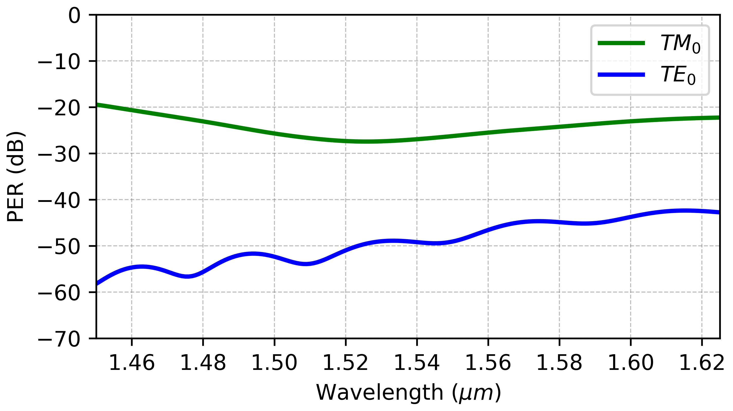
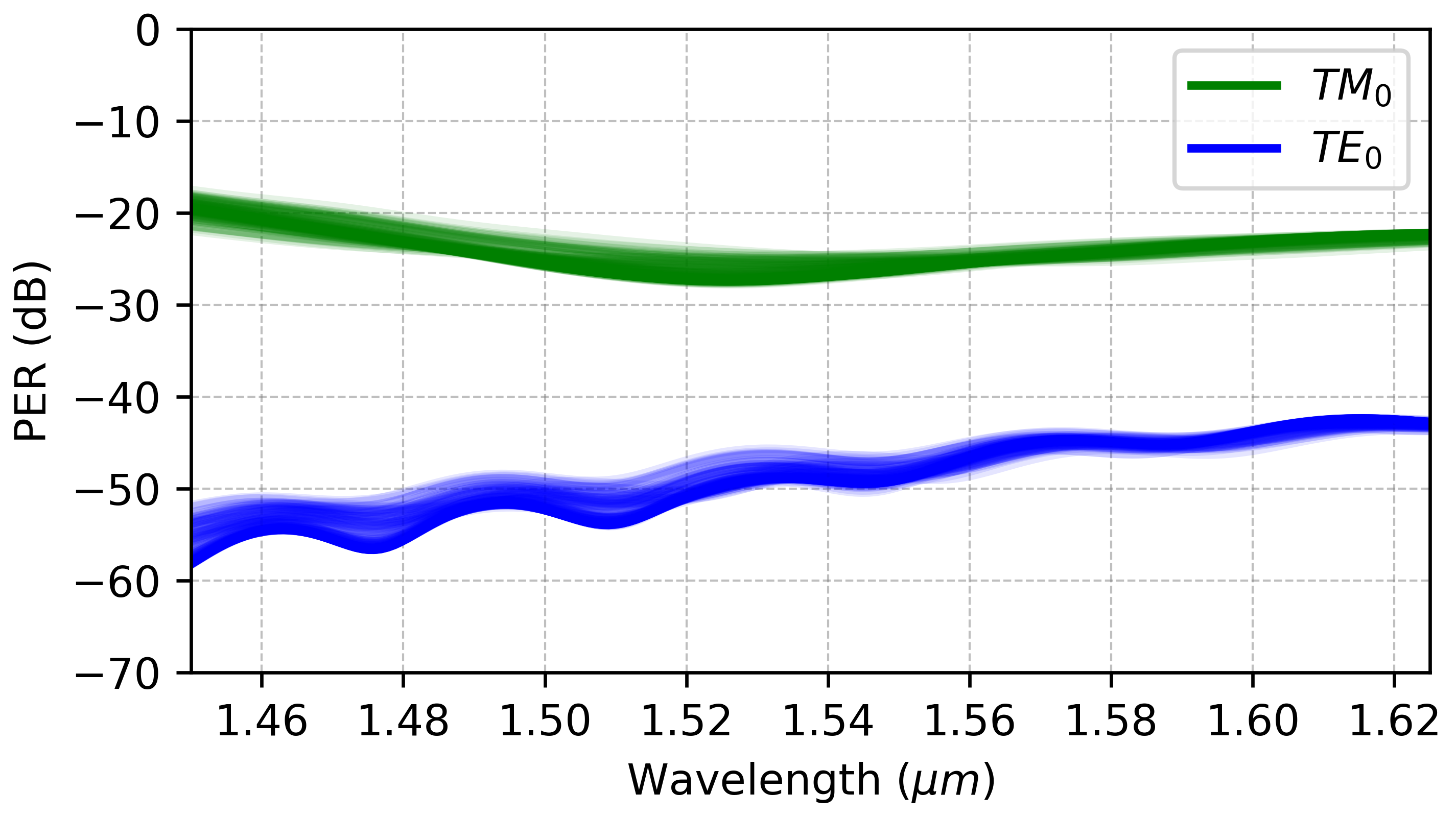
Performance: The nominal design presents a TE0-TM0 polarization conversion efficiency above above 80% from 1460 nm to 1625 nm and higher than 90% over a 120 nm wide range centered at the C band, which represents conversion losses <0.5 dB over the same range. In addition, the TE0-TE0 losses are <0.05 dB for all the bandwidth. The design also presents very low polarization extinction ratio (PER) for both polarizations below -40 dB.
Maturity level: II
LAYOUT
Black Box:

Pin specifications:
Pin No. |
Width (nm) |
|---|---|
0 |
500 |
1 |
500 |
2 |
500 |
FDTD & INTERCONNECT SIMULATION
This section describes the simulated performance of the building block, as well as the project conditions under which the simulations have been carried out. The results of this section have been obtained through Lumerical-Interconnect simulations for the performance of the complete device and precise 3D-FDTD simulations for the different subcomponents of the PDM. Convergence tests have been carried out to ensure maximum accuracy. Previous studies show negligible mode interaction with the BOX (Buried Oxide Layer).
Layer settings: The building block has been simulated in a SOI platform.
Layer |
Material |
Thickness |
|---|---|---|
Strip waveguide |
Si (dispersive) |
220 nm |
Slab waveguide |
Si (dispersive) |
90 nm |
Cladding |
SiO2 |
semi-infinite |
BOX |
SiO2 |
semi-infinite |
COMPACT MODEL
S-matrix settings: Lumerical Interconnect reads the compact model as an N-port building block with the following ports and modes:
Port No. |
Port name |
Mode |
Port location |
|---|---|---|---|
1 |
port 1 |
1 (TE0), 2 (TM0) |
Left |
2 |
port 2 |
1 (TE0), 2 (TM0), 3 (TE1) |
Left |
3 |
port 3 |
1 (TE0) |
Right |
The compact model contains the building-block performance at the following bandwidth:
Wavelength range |
|---|
1350-1750 nm |
FIGURES OF MERIT
Conversion efficiency
Conversion loss

Polarization Extinction Ratio (PER)

MONTE CARLO ANALYSIS
This section presents the Monte Carlo analysis performed to assess the effect of fabrication variations on the building block response.
SPECIFICATIONS
Besides the nominal design, four process corners have been calculated through 3D-FDTD simulations with the following width and thickness deviations (dw and dh, respectively).
Design |
dw (nm) |
dh (nm) |
|---|---|---|
nominal |
0 nm |
0 nm |
corner 1 |
+10 nm |
+5 nm |
corner 2 |
+10 nm |
-5 nm |
corner 3 |
-10 nm |
+5 nm |
corner 4 |
-10 nm |
-5 nm |
By interpolating from these designs, a Monte Carlo analysis has been performed using Gaussian statistical variation of dw and dh.
FIGURES OF MERIT
Conversion efficiency
Conversion loss

Polarization Extinction Ratio (PER)

MHT: MODE HYBRIDATION TAPER
DESCRIPTION
Summary: The MHT is a tapered polarization converter that offers an ultra-broadband and highly efficient solution for mode conversion between TM0 and TE1 modes. Polarization management is a key functionality in polarization diversity circuits and high-index contrast paltforms such as silicon with inherent birefringence.
Operational principle: The device works by converting the TM0 (TE1) signal to TE1(TM0) signal when light travels from Port 1 (Port 2) to Port 2 (Port 1), while leaving the TE0 signal unaffected.
Performance: The nominal design provides a TM0-TE1 conversion efficiency above 95% covering the S, C and L bands. Besides, the device ensures a conversion efficiency higher than 90% over a bandwidth of around 350 nm. Such high conversion efficiency represents conversion losses <0.22 dB. The device enables such mode conversion while keeping TE0-TE0 insertion losses below 0.15 dB. The TM0sub>0</sub> extinction ratio is below -18 dB over the whole range.
Maturity level: III-b
LAYOUT
Black Box:

Pin specifications:
Pin No. |
Width (nm) |
|---|---|
0 |
500 |
1 |
850 |
FDTD SIMULATION
This section describes the simulated performance of the building block, as well as the project conditions under which the simulations have been carried out. The results of this section have been obtained through precise 3D-FDTD simulations. Convergence tests have been carried out to ensure maximum accuracy.
Layer settings: The building block has been simulated in a SOI platform.
Layer |
Material |
Thickness |
|---|---|---|
Strip waveguide |
Si (dispersive) |
220 nm |
Slab waveguide |
Si (dispersive) |
90 nm |
Cladding |
SiO2 |
semi-infinite |
BOX |
SiO2 |
semi-infinite |
COMPACT MODEL
S-matrix settings: Lumerical Interconnect reads the compact model as an N-port building block with the following ports and modes:
Port No. |
Port name |
Mode |
Port location |
|---|---|---|---|
1 |
port 1 |
1 (TE0), 2 (TM0) |
Left |
2 |
port 2 |
1 (TE0), 2 (TM0), 3 (TE1), 5 (TE2) |
Right |
The compact model contains the building-block performance at the following bandwidth:
Wavelength range |
|---|
1350-1750 nm |
FIGURES OF MERIT
Conversion efficiency

Conversion loss

Extinction ratio

MONTE CARLO ANALYSIS
This section presents the Monte Carlo analysis performed to assess the effect of fabrication variations on the building block response.
SPECIFICATIONS
Besides the nominal design, four process corners have been calculated through 3D-FDTD simulations with the following width and thickness deviations (dw and dh, respectively).
Design |
dw (nm) |
dh (nm) |
|---|---|---|
nominal |
0 nm |
0 nm |
corner 1 |
+10 nm |
+5 nm |
corner 2 |
+10 nm |
-5 nm |
corner 3 |
-10 nm |
+5 nm |
corner 4 |
-10 nm |
-5 nm |
By interpolating from these designs, a Monte Carlo analysis has been performed using Gaussian statistical variation of dw and dh.
FIGURES OF MERIT
Conversion efficiency

Conversion loss

Extinction ratio

CROSSING
DESCRIPTION
Summary: Waveguide crossings are key building blocks to achieve high-volume and compact photonic circuits on a single chip. They enable the orthogonal intersection between two independent waveguides without interfering the signal transmission. This design works over a broad spectral range centered at the C band.
Operational principle: The design has four symmetrical ports. When light enters one of them, it will propagate to the in-front port with minimum losses and crosstalk with the adjacent ports.
Performance: The nominal design for TE polarization reaches minimum insertion losses of 0.03 dB. It also presents a broad operation band of 120 nm with insertion losses below 0.1 dB, crosstalk smaller than -37 dB and reflections below -30 dB. Moreover, insertion losses remain below 0.05 dB for C band.
Maturity level: III-b
LAYOUT
Black Box:

Pin specifications:
Pin No. |
Width (nm) |
|---|---|
0 |
450 |
1 |
450 |
2 |
450 |
3 |
450 |
FDTD SIMULATION
This section describes the simulated performance of the building block, as well as the project conditions under which the simulations have been carried out. The results of this section have been obtained through precise 3D-FDTD simulations. Convergence tests have been carried out to ensure maximum accuracy. Previous studies show negligible mode interaction with the BOX (Buried Oxide Layer).
Layer settings: The building block has been simulated in a SOI platform.
Layer |
Material |
Thickness |
|---|---|---|
Strip waveguide |
Si (dispersive) |
220 nm |
Cladding |
SiO2 |
semi-infinite |
BOX |
SiO2 |
semi-infinite |
COMPACT MODEL
S-matrix settings: Lumerical Interconnect reads the compact model as an N-port building block with the following ports and modes:
Port No. |
Port name |
Mode |
Port location |
|---|---|---|---|
1 |
port 1 |
1 (TE0) |
Left |
2 |
port 2 |
1 (TE0) |
Top |
3 |
port 3 |
1 (TE0) |
Bottom |
4 |
port 4 |
1 (TE0) |
Right |
The compact model contains the building-block performance at the following bandwidth:
Wavelength range |
|---|
1350-1750 nm |
FIGURES OF MERIT
Crosstalk

Insertion losses
Back reflections
MONTE CARLO ANALYSIS
This section presents the Monte Carlo analysis performed to assess the effect of fabrication variations on the building block response.
SPECIFICATIONS
Besides the nominal design, four process corners have been calculated through 3D-FDTD simulations with the following width and thickness deviations (dw and dh, respectively).
Design |
dw (nm) |
dh (nm) |
|---|---|---|
nominal |
0 nm |
0 nm |
corner 1 |
+10 nm |
+5 nm |
corner 2 |
+10 nm |
-5 nm |
corner 3 |
-10 nm |
+5 nm |
corner 4 |
-10 nm |
-5 nm |
By interpolating from these designs, a Monte Carlo analysis has been performed using Gaussian statistical variation of dw and dh.
FIGURES OF MERIT
Crosstalk

Insertion losses

Back reflections