
Whilst many applications (datacom, telecom, sensing, 5G, LIDAR, quantum computing…) could benefit from photonics adoption, when coming down to massive technology adoption scalability is a must, and integrated photonics is still making its way through.
So far integrated photonics have been developed under different platforms and design approaches in order to meet the needs of different applications ( e.g, quantum circuits exploit nonlinearities in waveguides whilst LIDAR circuits need to handle high power), often trading off performance on certain properties to benefit critical requirements.
As per the table below, Alcyon design combination of nanometric-thick silicon and SWG provides with an outstanding performance along most critical features, without needing to penalize one to favour another. Consequently, SWG silicon photonics designs can be transversal used to develop end application, which ends up on reusable technology that can reduce the time and cost from development time, fabrication, testing and optimization.
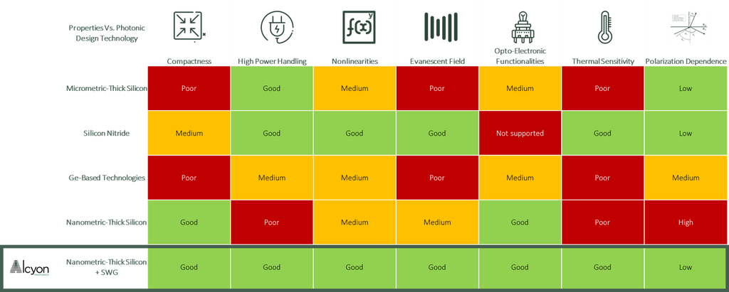
Whilst nanometric-thick silicon platform stands behind the good design behaviour in terms of compactness and opto-electronics. SWG design can claim its contribution to remarkably support key features such as like large evanescent field, low nonlinearity and low thermal sensitivity, following its confinement engineering capability. Additionally, SWG advanced metamaterial engineering of dispersion and birefringence enables performance far beyond other design techniques on critical application requirements such as ultra-wideband, ultra-narrowband and polarization management.
In summary, the combination of Nanometric-Thick Silicon and SWG supports consistently an outstanding performance for key features across most applications, which make of it a sound foundation stone to build a complete integrated photonic industry upon.